晶硅异质结光伏技术中透明导电氧化物靶材的研究进展与挑战

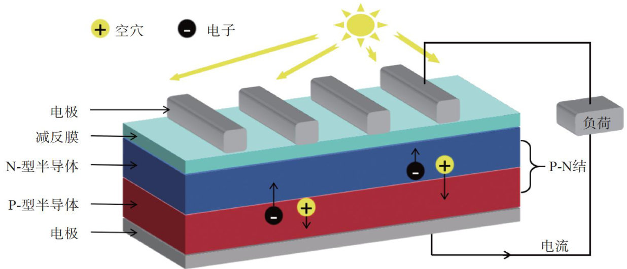
打开文本图片集
中图分类号:TM914.4 文献标志码:A
文章编号:2096-2983(2026)01-0054-10
Abstract: Crystaline silicon heterojunction (HJT) cells, recognized as third-generation photovoltaic technology, overcome the effciency limitations of PERC and TOPCon through low-temperature process compatibility, high open-circuit voltage, and superior temperature coefficients. Their efficiency ceiling andindustrialization process rely critically on multifunctional coordination within transparent conductive oxide (TCO) layers. High-mobility sputtering targets optimized via conduction band dispersion have enabled efficiency breakthroughs, while indium scarcity drives indium-free TCO development. Industrially, physical vapor deposition (PVD) dominates manufacturing due to high deposition rates and localized equipment, whereas reactive plasma deposition (RPD) achieves higher mobility through low-energy particle-induced lattice matching but faces constraints from imported equipment costs and low target utilization. Future advancements demand precise laboratory-toproduction mapping of target properties, with roll-to-roll (R2R) processintegration and perovskite/silicon tandem spectral synergy poised to propel HJT-based high-efficiency, low-carbon photovoltaic industrialization.
Keywords: crystalline silicon heterojunction cell; transparent conductive oxide thin film; sputring target
晶硅异质结(heterojunction,HJT)电池作为第三代高效光伏技术的代表,凭借其低温工艺兼容性、高开路电压及优异的温度系数,正逐步颠覆传统钝化发射极和背面电池(passivatedemitterand rearcell,PERC)与隧穿氧化层钝化接触(tunneloxidepassivated contact, TOPCon)电池技术的市场格局[1-3]其核心优势源于非晶硅/晶体硅(amorphoussilicon/crystallinesilicon heterojunction,a-Si/c-Si)HJT结构的创新设计:通过低于 200°C 的低温制造,规避了高温工艺导致的晶格畸变与热损伤,利用氢钝化非晶硅层将界面悬挂键密度控制在 1010/cm2 量级,显著抑制载流子复合,使少子寿命延长至5ms 以上[4-5]这一特性不仅支撑硅片厚度减薄至 120~130μm (材料损耗减少 15%~20% ,还通过双面对称结构与低温应力释放机制,实现薄片化硅片的机械良率超 98% 。(剩余18412字)