极紫外光学元件全频段面形误差检测与缺陷探测技术研究进展

打开文本图片集
关键词:先进光学制造;光学测量;面形检测;粗糙度检测;缺陷检测中图分类号:TN247 文献标识码:Adoi:10.37188/OPE.20253317.2661 CSTR:32169.14.OPE.20253317.2661
Research progress of full-spatial frequency error measurement and defect detection technology for extreme ultraviolet optical components
LI Jiahui 1,2 , KUANG Cuifang 1,2* , XU Yueshu²,BIAN Yinxu 2 , LIANG Jiadong²CUI Yudong 1,2 , LIU Xu1.²
(1. State Key Laboratory of Extreme Photonics and Instrumentation, Zhejiang University, Hangzhou 310027,China; 2. ZJU-Hangzhou Global Scientific and Technological Innovation Center, Zhejiang University, Hangzhou 311215,China) * Corresponding author,E-mail: cfkuang@zju. edu. cn
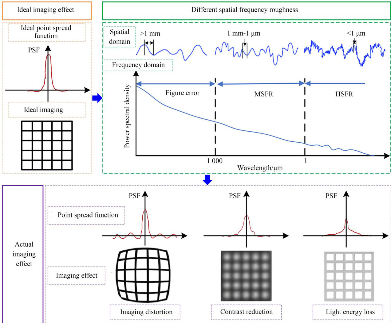
Abstract: Extreme ultraviolet lithography,a pivotal technology in semiconductor manufacturing,imposes atomic-scale precision requirements on optical surfaces and necessitates negligible surface and subsurface damage.This paper addresses ultra-precision fabrication of optical components by first elucidating the mechanisms by which material properties and manufacturing processes induce surface erors.Technical challenges and recent advances in measuring surface errors across spatial scales are then analyzed.For low-spatial-frequency figure errors,emphasis is placed on absolute measurement methods and sub-aperture stitching techniques.For mid-to high-spatial-frequency roughness,developments inwhite-light interferometry microscopy, atomic force microscopy,and superresolution white-light interferometry are reviewed. To meet multi-modal characterization requirements for surface and subsurface defects,the advantages and limitations of complementary detection methods-including electron microscopy,interferometry,scanning probe techniques, and scattering approaches-are comparatively assessed. Finally,against the backdrop of prevailing technical bottlenecks and the demand for high-performance optics,future directions are delineated,highlighting intelligent measurement systems,multi-physical coupled characterization,and in-situ monitoring.This analysis is intended to serve as a technical reference to support domestic production of critical equipment components.
Key words: advanced optical manufacturing; optical measurement; surface metrology; surface roughnessmeasurement;defectmeasurement
1引言
光刻机是集成电路的关键制造装备,其光刻分辨率直接决定了芯片制造的工艺极限。(剩余54755字)